
Semiconductors & Coating
6N copper for sputter targets and thin-film processes — SEMI-qualified, full batch traceability.
Semiconductor-grade sourcing leaves no room for contamination.
Sub-ppm contamination risk
A single metallic impurity at parts-per-billion level can compromise an entire wafer lot. Standard copper supply chains lack the analytical depth to detect this.
SEMI Standards compliance
Meeting SEMI C1.15 and related fab specifications requires coordinated testing protocols that most metal traders do not support.
Traceability from melt to fab
Fabs require complete traceability per wafer lot. Without melt-to-delivery documentation, incoming inspection becomes a bottleneck.
Cleanroom-ready copper with full melt traceability.
GDMS and mass spectrometric dual analysis
Every batch is analyzed at ppb level using Glow Discharge Mass Spectrometry alongside mass spectrometric trace element analysis. Impurity profiles are documented per SEMI standards.
SEMI-aligned documentation
Mass spectrometric analysis with sub-ppm resolution. All documentation is prepared for direct integration into your fab's quality system.
Vacuum-sealed, numbered bars
Each copper bar is individually numbered, vacuum-packed and traceable to its specific melt. No cross-contamination risk during transport.
Qualify semiconductor-grade copper for your fab
Receive sample bars or powder with GDMS analysis at ppb resolution — validated for cleanroom integration and incoming inspection.
How copper enables advanced semiconductor processes
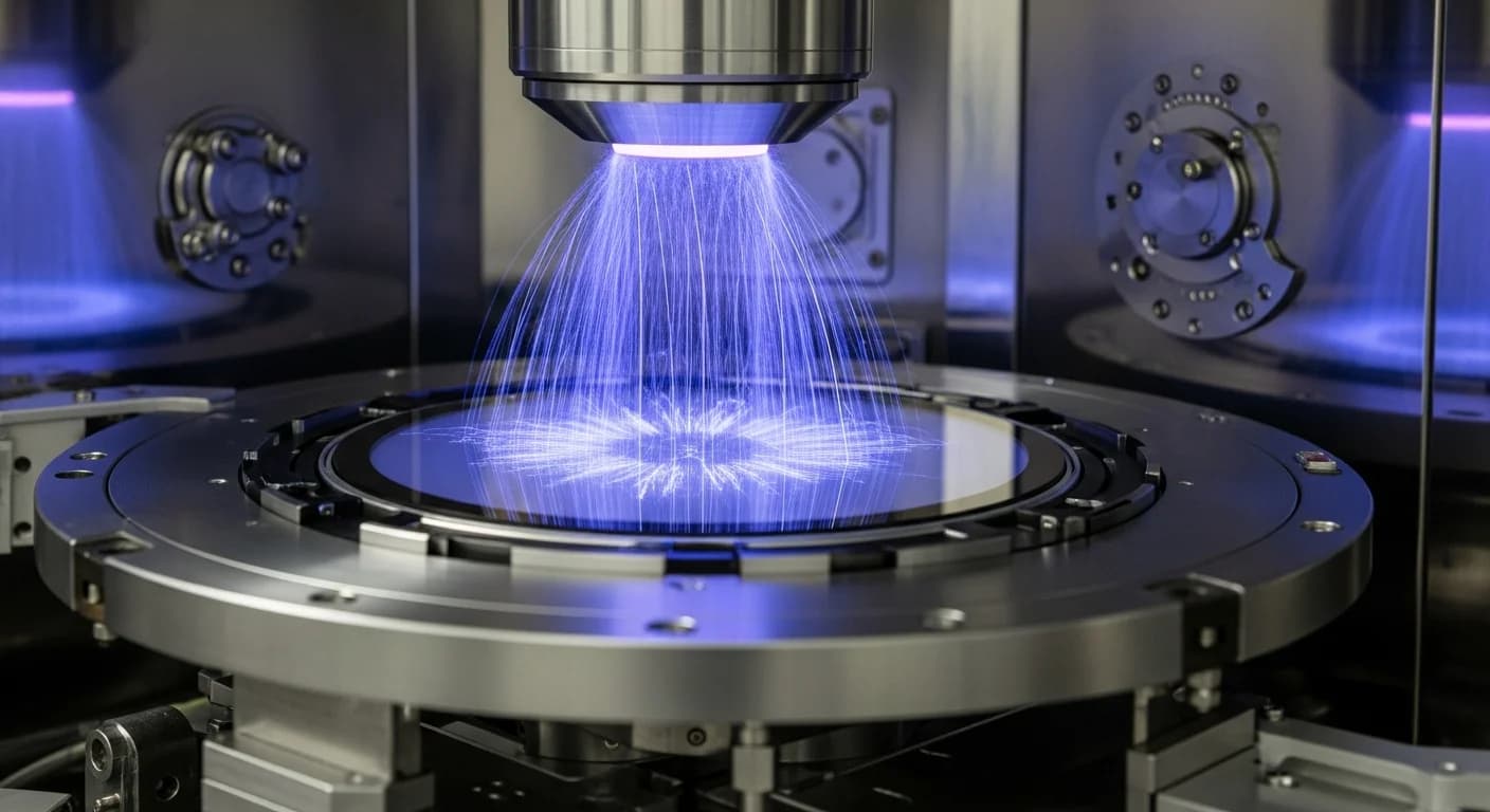
PVD/CVD Thin-Film Coatings
6N copper bars are machined into high-purity sputter targets for physical vapor deposition in semiconductor fabs. Sub-ppm impurity levels ensure defect-free copper seed layers on 300 mm wafers, critical for interconnect reliability at advanced nodes.

Wafer-Level Copper Bonding
Ultra-pure copper powder is used in thermocompression bonding and copper pillar bump formation for 3D IC stacking. Ultradisperse grain structure ensures void-free bonds with high shear strength at the die-to-die interface.
Compliance for semiconductor fabrication
Certified quality management across all manufacturer partners.
Full REACH compliance for the European market.
Verified supply chain per Conflict Minerals Policy.
Certificate of Analysis with complete analytics for every batch.
Materials for semiconductors.
Copper Bar 6N
Individually numbered 6N bars for sputter target blanks. Mass spectrometry verified purity prevents outgassing during PVD processes in vacuum chambers.
Copper Powder 6N
High-purity powder for advanced coating applications, paste formulations and research-scale deposition experiments requiring 6N feedstock.
Semiconductors & Coating
6N copper for sputter targets and thin-film processes — SEMI-qualified, full batch traceability.
Total metallic impurities below 1 ppm, verified by GDMS. Individual elements (Fe, Ag, Pb) at sub-100 ppb levels. Full impurity profile on the CoA.
Yes. Our 6N bars are used as blanks by target manufacturers. Dimensions and surface finish can be specified to match your bonding requirements.
Each bar is vacuum-sealed individually with inert atmosphere. Transport uses dedicated containers — no co-shipment with other metals.
More industries requiring high-purity copper.
Source semiconductor-grade copper.
Request bars or powder with GDMS analysis and SEMI-aligned documentation.
Start request